|
MICRO SCALE PATTERN TRANSFER WITHOUT PHOTOLITHOGRAPHY OF SUBSTRATES S. Roy and I. Schönenberger School of Chemical Engineering and Advanced Materials and Institute of Nanoscale Science and Technology University of Newcastle, Merz Court Newcastle upon Tyne, NE1 7RU, U.K |

|
In this work we have developed a process to transfer micro scale patterns on a fully exposed (un-patterned) substrate. The method uses electrochemical means and a specialised electrochemical reactor for pattern transfer. This process uses a metallic material with a resist pattern, which serves as an electrochemical tool. The substrate, which is fully exposed, is placed facing the tool, within close proximity. The tool and the substrate are electrically connected so that the tool is the cathode and the substrate is the anode. Electrolyte is pumped through the system to deliver fresh solution to the anode and cathode as well as remove reaction by products.
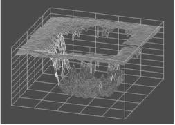
Our initial experiments, involving copper as the tool as well as substrate material, showed that micro scale patterns could be transferred with good reproducibility. In our reactor, they were placed within a distance of 500 mm. We have successfully transferred micro patterns which are significantly smaller than the electrode gap, namely, 50, 100 and 200 mm. A specimen 3-D optical profile of a 100 mm x 100 mm square pattern obtained by this process is shown in the following figure. The steep walls and cubic shape demonstrate the feasibility of the process. Since a single tool can be used to transfer a pattern numerous times, this opens the the possibility of greatly reducing the use of photolithography for pattern transfer on to metallic substrates.